 | –≠–ª–µ–∫—Ç—Ä–æ–Ω–Ω—ã–π –∫–æ–º–ø–æ–Ω–µ–Ω—Ç: MC34063AC | –°–∫–∞—á–∞—Ç—å:  PDF PDF  ZIP ZIP |
MC34063A
DC-DC CONVERTER CONTROL CIRCUITS
Æ
April 2000
s
OUTPUT SWITCH CURRENT IN EXCESS OF
1.5A
s
2% REFERENCE ACCURACY
s
LOW QUIESCENT CURRENT: 2.5mA (TYP.)
s
OPERATING FROM 3V TO 40V
s
FREQUENCY OPERATION TO 100KHz
s
ACTIVE CURRENT LIMITING
DESCRIPTION
The MC34063A series is a monolithic control
circuit delivering the main functions for DC-DC
voltage converting.
The device contains an internal temperature
compensated reference, comparator, duty cycle
controlled oscillator with an active current limit
circuit, driver and high current output switch.
Output voltage is adjustable through two external
resistors with a 2% reference accuracy.
Employing
a
minimum
number of
external
components the MC34063A devices series is
designed
for
Step-Down,
Step-Up
and
Voltage-Inverting applications.
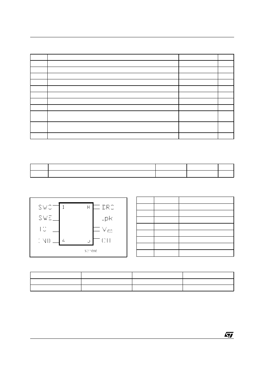
BLOCK DIAGRAM
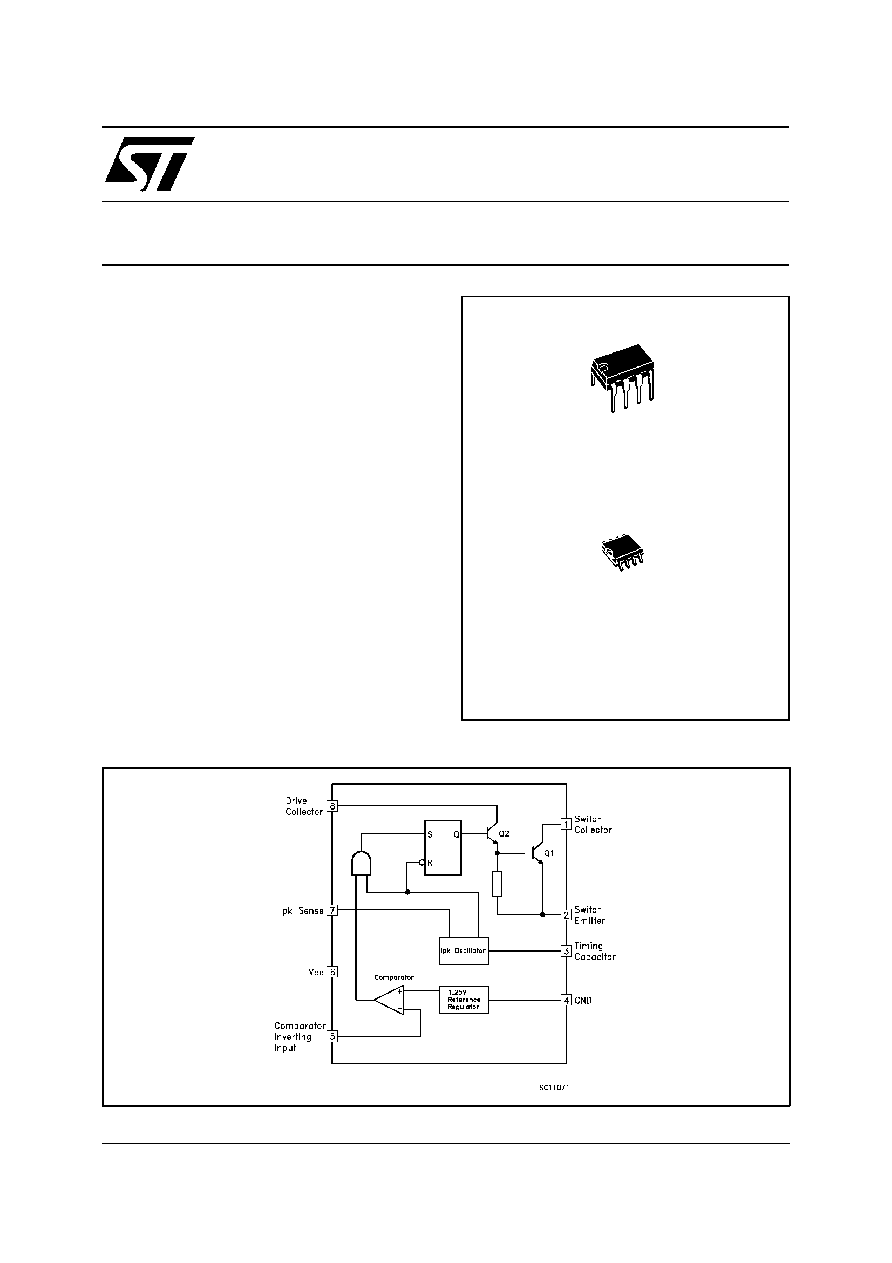
DIP-8
SO-8
1/15
ABSOLUTE MAXIMUM RATINGS
Symbol
Parameter
Value
Unit
V
CC
Power Supply Voltage
50
V
V
ir
Comparator Input Voltage Range
-0.3 t o 40
V
V
SWC
Switch Collector Voltage
40
V
V
SWE
Switch Emitter Voltage (VSWC = 40V)
40
V
V
CE
Switch Emitter to Collector Voltage
40
V
V
d c
Driver Collector Voltage
40
V
I
dc
Driver Collector Current
100
mA
I
SW
Switch Current
1.5
A
P
tot
Power Dissipation at T
amb
= 25
o
C (for Plastic Package)
(for SOIC Package)
1.25
0.625
W
T
op
Operating Ambient Temperature Range (for AC SERIES)
(for AB SERIES)
0 to 70
- 40 to 85
o
C
o
C
T
st g
Storage Temperature Range
- 40 to 150
o
C
Absolute Maximum Rating are those values beyond which damage to the device may occur.
Functional operation under these condition is not implied.
THERMAL DATA
Symbol
Parameter
DIP-8
SO-8
Unit
R
thj- amb
Thermal Resistance Junction-ambient (*)
Max
100
160
o
C/W
(*) This value depends from thermal design of PCB on which the device is mounted.
ORDERING NUMBERS
Type
DIP-8
SO-8
SO-8 (tape & reel)
MC34063AB
MC34063ABN
MC34063ABD
MC34063ABD-TR
MC34063AC
MC34063ACN
MC34063ACD
MC34063ACD-TR
CONNECTION DIAGRAM (top view)
PIN CONNECTIONS
Pin No
Symbol
Name and Function
1
SWC
Switch Collector
2
SW E
Switch Emitter
3
T C
Timing Capacitor
4
GND
Ground
5
CII
Comparator Inverting Input
6
V
CC
Voltage Supply
7
I
pk
I
pk
Sense
8
DRC
Voltage Driver Collector
MC34063A
2/15
ELECTRICAL CHARACTERISTICS (Refer to the test circuits, V
CC
= 5V, T
a
= T
LOW
to T
HIGH
, unless
otherwise specified, see note 2)
OSCILLATOR
Symbol
Parameter
Test Conditions
Min.
Typ.
Max.
Unit
f
OSC
Frequency
V
pin5
= 0 V
C
T
= 1 nF
T
a
= 25
o
C
24
33
42
KHz
I
ch g
Charge Currernt
V
CC
= 5 to 40 V
T
a
= 25
o
C
24
33
42
µ
A
I
dischg
Discharge Current
V
CC
= 5 to 40 V
T
a
= 25
o
C
140
200
260
µ
A
I
d is ch g
/I
chg
Discharge to Charge
Current Ratio
Pin 7 = V
CC
T
a
= 25
o
C
5.2
6.2
7.5
V
i pk( sense)
Current Limit Sense Voltage
I
chg
= I
dischg
T
a
= 25
o
C
250
300
350
mV
OUTPUT SWITCH
Symbol
Parameter
Test Conditions
Min.
Typ.
Max.
Unit
V
CE(sat)
Saturation Voltage,
Darlington Connection
I
SW
= 1 A
Pins 1, 8 connected
1
1.3
V
V
CE(sat)
Saturation Voltage
I
SW
= 1 A
R
pin8
= 82
to V
CC
,
Forced
~ 20
0.45
0.7
V
h
F E
DC Current Gain
I
SW
= 1 A
V
CE
= 5 V
T
a
= 25
o
C
50
120
I
C( off)
Collector Off-State Current
V
CE
= 40 V
0.01
100
µ
A
COMPARATOR
Symbol
Parameter
Test Conditions
Min.
Typ.
Max.
Unit
V
t h
Threshold Voltage
T
a
= 25
o
C
T
a
= T
LOW
to T
HIGH
1.225
1.21
1.25
1. 275
1.29
V
V
Reg
li ne
Threshold Voltage Line
Regulation
V
CC
= 3 to 40 V
1
5
mV
I
I B
Input Bias Current
V
IN
= 0 V
-5
-400
nA
TOTAL DEVICE
Symbol
Parameter
Test Conditions
Min.
Typ.
Max.
Unit
I
CC
Supply Current
V
CC
= 5 to 40 V
C
T
= 1 nF
Pin 7 = V
CC
V
pin5
> V
th
Pin 2 = GND
Remaining pins open
2.5
4
mA
NOTES:
1) Maximum package power dissipation limit must be observed.
2) T
LOW
= 0
o
C, T
HIGH
= 70
o
C (AC series); T
LOW
= -40
o
C, T
HIGH
= 85
o
C (AB series).
3) If Darlington configuration is not used, care must be taken to avoid deep saturation of output switch. The resulting switch-off time may be
adversely affected. In a Darlington configuration the following output driver condition is suggested:
Forced
of output current switch = I
COUTPUT
/(I
CDRIVER
- 1mA*)
10
* Current less due to a built in 1K
antileakage resistor.
MC34063A
3/15
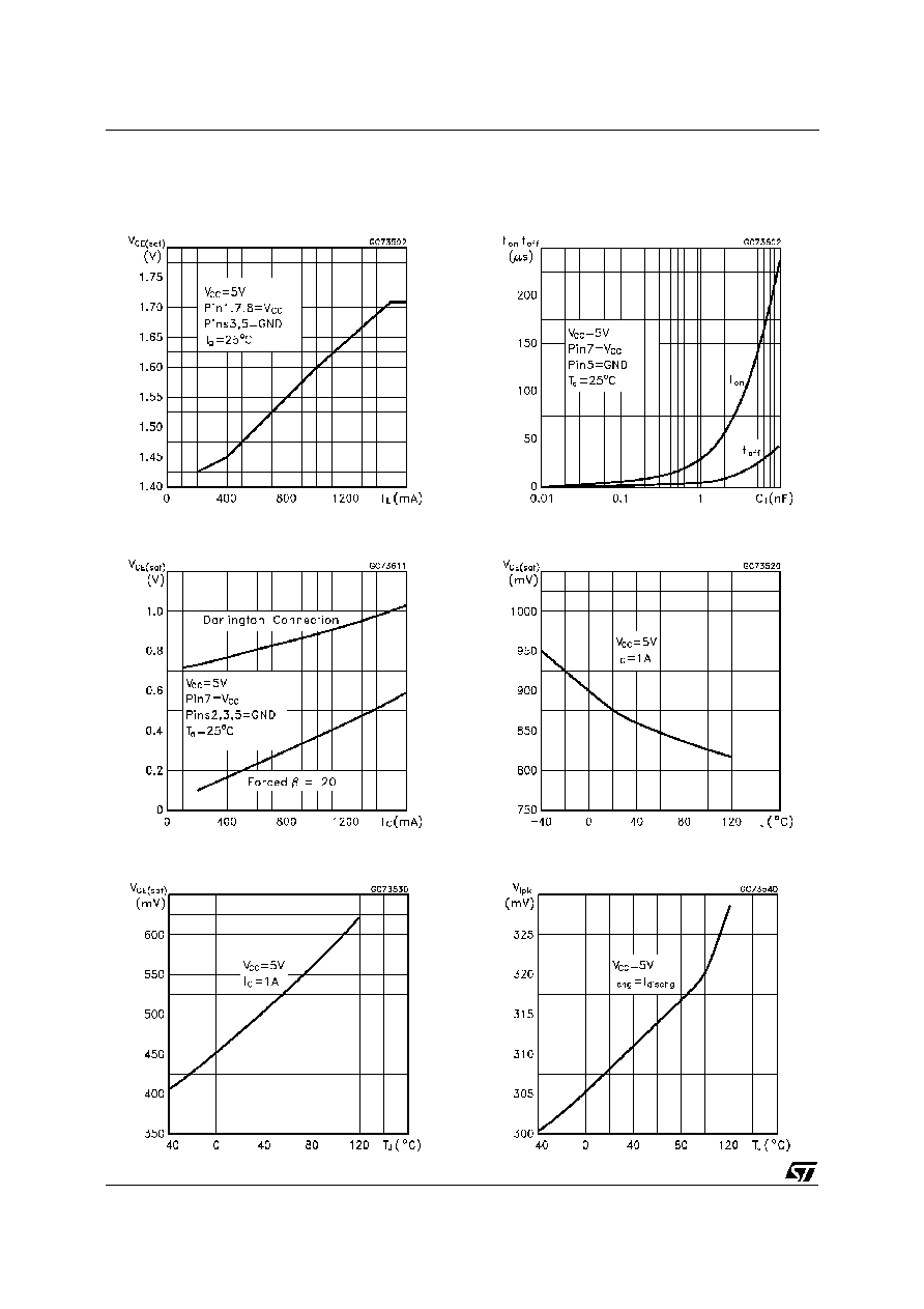
Common Emitter Configuration Output Switch
Saturation Voltage vs Collector Current
Power Collector Emitter Saturation Voltage
(V
CE(sat)
) vs Temperature
Darlington Configuration Collector Emitter
Saturation Voltage (V
CE(sat)
) vs Temperature
Current Limit Sense Voltage Voltage (V
ipk
) vs
Temperature
Emitter Follower Configuration Output Saturation
Voltage vs Emitter Current
Output Switch ON-OFF Time vs Oscillator
Timing Capacitor
TYPICAL ELECTRICAL CHARACTERISTICS
MC34063A
4/15
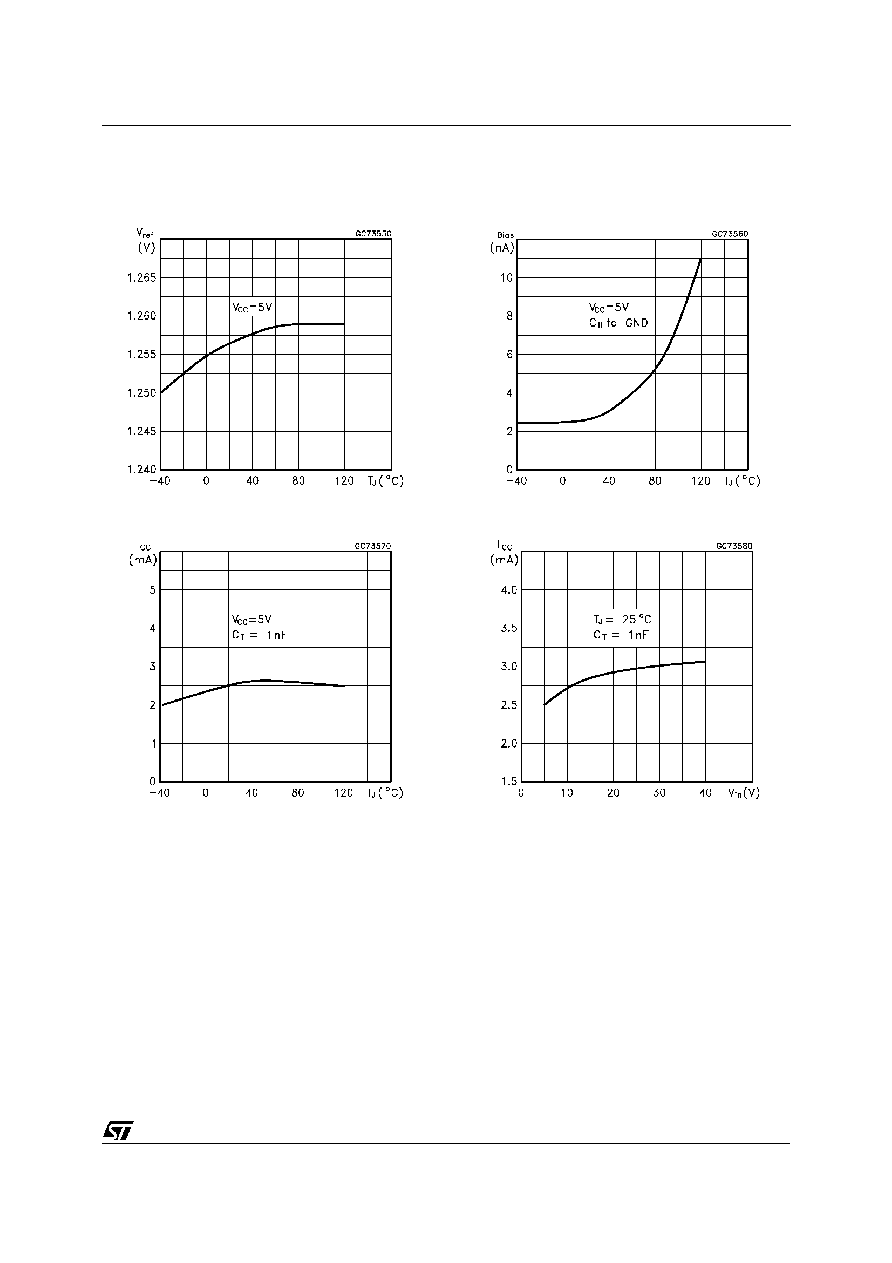
Supply Current vs Temperature
Supply Current vs Input Voltage
Reference Voltage vs Temperature
Bias Current vs Temperature
TYPICAL ELECTRICAL CHARACTERISTICS (Continued)
MC34063A
5/15